*Corresponding Author:
Liu S,
State Key Laboratory of Particle Detection and Electronics, Institute of High Energy Physics, Chinese Academy of Sciences, University of Chinese Academy of Sciences, Beijing 100049,China
E-mail: liusl@ihep.ac.cn
Sun Z,
State Key Laboratory of Particle Detection and Electronics, Institute of High Energy Physics, Chinese Academy of Sciences, Spallation Neutron Source Science Center, University of Chinese Academy of Sciences, Beijing 100049, China
E-mail: sunzj@ihep.ac.cn
Abstract
The Design of the Emission Layer for Electron Multipliers published Nanoscale Reseach Letters 16, 151 (2021) https://doi.org/10.1186/s11671-021-03606-y. The main corresponding author is Shulin Liu (liusl@ihep.ac.cn), the first author is Yuman Wang. This paper comprehensively introduces the preparation method and design principle, test instrument, test method, analysis method and other aspects of the design of the emission layer for electron multiplier. This short review reviews the innovations in these aspects, such as the design principle of sandwich structure, the preparation method of atomic layer deposition, the structure of spherical SEE test equipment, the method of low-energy secondary electron neutralization, the alternative use of XPS and etching to study high SEE materials, etc.
Keywords
Al2O3; Electron multipliers; MgO; Secondary electron emission coefficient.
Introduction
The gain of the electron multiplier is closely related to the Secondary Electron Emission coefficient (SEE) and the thickness of the emitter layer, so it is very important to study their related properties. According to the working principle and the idea of limit, this paper proposes three design targets for the preparation of excellent emission layer: 1. Thinner film; 2. Higher SEE; 3. more stable working performance. The SEE value is closely related to the thickness of the emission layer. According to the idea of limit, as shown in Figure 1(a),1(b), if the emission layer is too thick, the gain of the electron multiplier will be saturated in advance due to the reason that the conductive layer cannot immediately supplement the electrons lost by the emission layer when the secondary electron avalanche occurs. As shown in Figure 1(c), if the emission layer is very thin, a lower SEE value will result in a lower gain of the electron multiplier.
According to the SEE of related materials, although the SEE of MgO is higher than that of Al2O3[1,2], Al2O3 is usually selected as the emission layer in the electron multiplier rather than MgO in practical processes. The main reasons are as follows: Firstly, MgO is easily deliquescent into Mg(OH)2, Mg2(OH)2和MgCO3, which will cause the SEE of the emission layer to be reduced to the level of Al2O3. Secondly, the film is very thick (35 nm) when saturated SEE is ob- tained by MgO, so that the conductivity layer cannot replenish charge to the surface of the emission layer in time. Third, the properties of Al2O3 can maintain long-term stability in the atmosphere; Fourthly the preparation process of Al2O3 is simpler than MgO.

Figure 1: Includes the emission layer and the conductive layer, showing the working process of the electron multiplier. (a):Schematic diagram of electron beam and current when the emission layer thickness is suitable.(b):Schematic diagram of electron beam and current when the emission layer is too thick.(c): Schematic diagram of electron beam and current when the emission layer is too thin.
In order to measure the SEE level of materials, many laboratories around the world have established their own special measurement equipment, including Argonne Laboratory [2], Stanford Linear Accelerator Center [3], University of Utah [4], Princeton University [5], ONERA/DESP [6], University of Science and Technology of China, Xi ‘an Jiaotong University and University of Electronic Science and Technology of China. SEE measurement equipment built for emission layer materials is dominated by Argonne Laboratory, which undertook the development of emission layer in LAPPD project, and adopts a hemispherical structure to collect secondary electrons. The maximum energy of incident electrons configured with electron gun is 1000 eV, but sample charging limits the ability to measure MgO samples [2].At present, the main SEE physical model is Dionne model [7,8]. However, the bilayer model [9,10].
Proposed in the existing literature is not applicable to the experimental results of multilayer films, although it has been further modified. In order to better evaluate the SEE value of thin films, a classification method is adopted in the field of micro-discharge suppression [3], but it is not applicable to films with high SEE value.
This paper solves the following problems: how to build an equipment to measure SEE of emission layer material, improve the accuracy of the test and solve the measurement problem of MgO; How to prevent deliquescence of MgO; How to prepare the emission layer film material with suitable thickness for electron multiplier, and what are the design principles? How to better explain multi-layer experimental phenomena under the condition that the current theoretical model is not applicable; How to better evaluate the films with high SEE values when the current SEE classification is not applicable? what tools to use for characterization analysis of high SEE materials.
The Innovation and Development of This Paper
It is well known that secondary electron emission occurs between a few nanometers and tens of nanometers deep in the material. Atomic Layer Deposition (ALD) can control the thickness and composition of atomic film to prepare high quality films [11,12]. Therefore, ALD is selected as an important preparation method to study the emission layer thickness in this paper [9,13-15] Figure 2.
Al2O3 and MgO films are usually selected as emission layers for electron multipliers because of the higher SEE of these two materi- als. MgO deliquesce easily into MgCO3 and Mg2(OH)2 CO3, which resulted in the decrease of SEE. SEE of Al2O3 is lower than that of MgO, but the performance of Al2O3is stable. Research shows that the final products of deliquescent MgO are mainly Mg2 (OH)2CO3and MgCO3[16]. Therefore, the deliquescent depth of MgO can be re- flected by detecting C atomic concentration at different depths of materials. In this paper, Ar ion beam was used to etch the surface of the material and X-ray Photoelectron Spectroscopy (XPS) was used to analyze it. In the alternating process, time was controlled to con- trol the etch depth, and the relative atomic concentration percentage changes of C and Mg elements could be obtained with XPS. When XPS cannot provide the relative concentration percentage of C ele- ment, the ion etching depth is the deliquescence depth of MgO. This paper show that the deliquescence depth of MgO is about 3.8 nm. The computational reasoning is as follow Figure 3.
It can be seen from Figure 2 that the Si element was measured at 180 s, which means that most of the grown MgO has been etched away, and the remaining MgO is mixed with Si, and the rate of etch- ing MgO can be roughly calculated.
Etching rate MgO=ThicknessMgO/Etching timeMgO=11.58 nm/180 s=0.643 Å/s
Here, we approximate the etching rate of deliquescence materials such as Mg2(OH)2CO3to that of MgO, and no C element is contained at 60 s, so it can be considered that this etching depth is the deliquescence depth.
Etching ThicknessMg2(OH)2CO3≈Etching ThicknessMgO=Etching rateMgO*Etching timeMgO=0.643 Å/s*60 s≈3.85 nm

Figure 2: The 11nm MgO etching time and the measured relative content of Mg and Si elements.
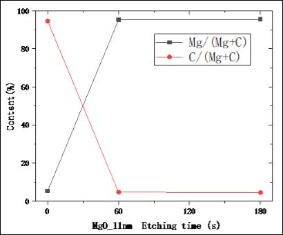
Figure 3: The 11nm MgO etching time and the measured relative content of Mg and C elements.
In this paper, a spherical system is designed to test the SEE of materials to ensure adequate collection of secondary electrons and thus help improve the accuracy of SEE measurements. A low energy secondary electron beam is proposed to replace the low energy electron beam to neutralize the positive charge generated on the surface of the measured material, so as to obtain the real SEE value of the measured material (such as MgO and Al2O3), thus avoiding the disadvantages of adding additional neutralization dose and neutralization time [6,17]. This method is convenient and cost saving. And successfully solved the problem of surface electrified and inaccurate measurement in MgO testing process.
In this paper, the incident electron energy is divided into low energy region, medium energy region and high energy region by comparing SEE under the nearest incident electron energy as a standard. Studies have found that the incident electron in the intermediate energy region can obtain the optimal SEE value, which is different from the classification standard in the field of inhibiting micro-discharge [3]. Based on this standard, this paper conducts in-depth research and obtains empirical formulas of SEE value related to emission layer film thickness for four different materials such as Al2O3, MgO, MgO/ Al2O3, Al2O3/MgOunder optimal conditions.
This paper found that the composite film growing Al2O3 film first and then MgO film has a better effect. When the composite film is very thin, the saturated SEE level of MgO can be reached. This solves the problem that the conductivity layer cannot fully replenish the charge due to the thickness of the MgO film. At the same time, it is found that growing Al2O3 film after growing MgO film can prevent deliquescence of MgO film and keep high SEE level of MgO film for a long time. This paper found that the preparation of 1 nm Al2O3 film can resist the external environment of MgO erosion damage; The preparation of 0.3 nm Al2O3can further improve the saturation SEE level of MgO.
In view of the experimental phenomenon that the thickness of the same top layer material is different when it reaches the saturation SEE level in different bottom layers of the bilayer material structure, this paper puts forward the concept of “transition layer” to better explain the material characteristics of the design. XPS and ion etching were used to analyze the element content of multilayer materials, and the relative content of element C was used as the standard element of deliquescence depth and moisture-proof solution thickness. Here we only analyze the relative content of the two elements by scanning the broad spectrum of XPS, and do not scan the narrow spectrum of each element. For the detailed analysis, see this paper Figure 4.

Figure 4: New emission layer structure. (a): Al2O3/MgO/Al2O3 Schematic diagram of each functional layer structure. (b): Al2O3/MgO/Al2O3 structure diagram ex- plained by XPS and “transition layer”.
With the help of transition layer thought and experiment and aux- iliary calculation, this paper puts forward the technological design idea of preparing new emission layer. The emission layer of sandwich structure is designed by using the design principle of materials with thin transition layer as buffer layer, high SEE material as main layer and non-deliquescent material as protective layer, as shown in Figure 4. In other words, a 5~9 nm MgO main layer is grown on 2~3 nm Al2O3buffer layer, and then 1 nmAl2O3 protective layer is grown, so as to solve the above problems related to the preparation of emission layer in electron multiplier tube by MgO. Experimental results show that the emission layer films with this structure can maintain a high SEE value for a long time. This new structure can also be used in oth- er devices such as Channel Electron Multiplier (CEM) and separate puller, which has a wide application space.The explored R & D route can help us develop more excellent emission layer films faster and more purposefully, as shown in Figure 5.
Conclusion
This paper proposes that the idea of choosing athinner “transition layer” as the buffer layer can provide some inspiration for preparing thinner and higher SEE emission layers. The sandwich structure provides an effective way to prepare a more stable emission layer, and the optimal SEE and thickness formula can be obtained by dividing the incident electron energy by the “nearest neighbor” SEE primary electron energy ratio to design the thickness of various materials. We hope to develop emission layers with more stable material structure, higher SEE and better film thickness through the path explored as shown in figure 5, and strive to promote the application in many aspects of electron multiplication field, such as photomultiplier tubes, time of flight mass spectrometry, night vision instrument and other instruments.

Figure 5: Emission layer R&D Roadmap.
Acknowledgments
This work was supported by the National Natural Science Foundation of China (Grant Nos.11535014, 11675278, 11975017 and 12175254), the State Key Laboratory of Particle Detection and Electronics (SKLPDE-ZZ- 202015), the National Key R&D Program of China (Grant No.2021YFA1600703), and Youth Innovation Promotion Association CAS, China.
References
- Guo J, Wang D, Wen K, Xu Y, Zhu X, et al. (2020) Theoretical and ex- perimental investigation of secondary electron emission characteristics of MgO coating produced by atomic layer AIP Advances Ceram- ics International 46: 8352-8357.
- Jokela SJ, Veryovkin IV, Zinovev AV, Elam JW, Mane AU, et al. (2012) Secondary Electron Yield of Emissive Materials for Large-Area Mi- cro-Channel Plate Detectors: Surface Composition and Film Thickness Physics Procedia 37: 740-747.
- Pivi MV, King FK, Kirby RE, Raubenheimer TO, Stupakov G, et (2008) Sharp reduction of the secondary electron emission yield from grooved surfaces 104: 2120.
- https://digitalcommons.usu.edu/cgi/viewcontent.cgi?article=3094&con-text=etd
- Dunaevsky A, Raitses Y, Fisch NJ (2003) Secondary electron emission from dielectric materials of a Hall thruster with segmented electrodes. Physics of Plasmas 10: 2574-2577.
- Belhaj M, Tondu T, Inguimbert V (2011) Effect of the incident electron fluence on the electron emission yield of polycrystalline Applied Surface Science 257: 4593-4596.
- Gerald DF (1973) Effects of secondary electron scattering on secondary emission yield curves. Journal of Applied Physics 44: 5361-5364.
- Dionne GF (1975) Origin of secondary-electron-emission yield-curve pa- Journal of Applied Physics 46: 3347-3347.
- Cao W, Wang B, Yang Y, Zhu B, Guo J, et al. (2021) Secondary electron emission characteristics of the Al2O3/MgO double-layer structure pre- pared by atomic layer deposition. Ceramics International 47: 9866-9872.
- Wang D, He Y, Guo J, Cai Y, Ye M (2021) Investigation on secondary elec- tron emission characteristics of double-layer Journal of Applied Physics 129: 093304.
- Tao J, Lu HL, Gu Y, Ma HP, Li X, et al. (2019) Investigation of growth characteristics, compositions, and properties of atomic layer deposited amorphous Zn-doped Ga2O3 films. Applied Surface Science 476: 733- 740.
- Tao JJ, Ma HP, Yuan KP, Gu Y, Lian JW, et al. (2020) Modification of 1D TiO2 nanowires with GaOxNy by atomic layer deposition for TiO2@ GaOxNy core-shell nanowires with enhanced photoelectrochemical per- Nanoscale 12: 7159-7173.
- Mane AU, Tong WM, Brodie AD, McCord MA, Elam JW (2014) Atomic layer deposition of nanostructured tunable resistance coatings: Growth, characterization, and electrical properties. ECS Transactions 64: 3.
- Elam JW, Mane AU, Libera JA, Hryn JN, Siegmund OH, et al. (2013) Synthesis, characterization, and application of tunable resistance coatings prepared by Atomic Layer Deposition. ECS Transactions 58: 249.
- Lu J, Elam JW, Stair PC (2016) Atomic layer deposition-Sequential self-limiting surface reactions for advanced catalyst “bottom-up” synthe- Surface Science Reports71: 410-472.
- Rong-Zhen L (2011) Research on Moisture Absorption and Deliquescence Behavior of Single Crystal MgO Polishing Substrate. Development Inno- vation of Machinery Electrical Products.
- Belhaj M, Tondu T, Inguimbert V, Chardon JP (2009) A Kelvin probe based method for measuring the electron emission yield of insulators and insulated conductors subjected to electron irradiation. Journal of Physics D Applied Physics 42: 105309.
Citation: Wang Y, Liu S, Yan B, Wen K, Qi M, et al. (2022) A Short Review on the Published Paper: The Design of the Emission Layer for Electron Multipliers. J NanosciNanomedNanobio 5:13.
Copyright: © 2022 Wang Y, et al. This is an open-access article distributed under the terms of the Creative Commons Attribution License, which permits unrestricted use, distribution, and re- production in any medium, provided the original author and source are credited.